
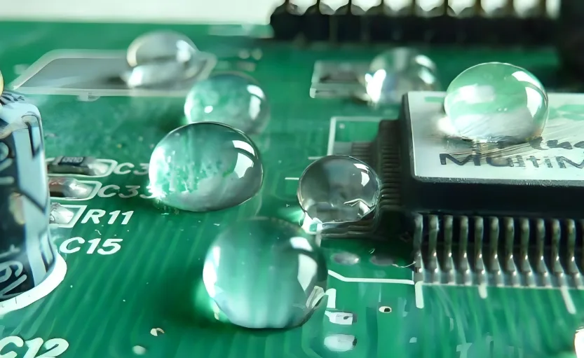
In today’s world, where electronic devices are becoming increasingly ubiquitous—from smartwatches to outdoor sensors—our expectations for durability and performance continue to rise. Among these performance requirements, waterproofing has become a critical specification for many devices. At the core of achieving water resistance in electronics lies the waterproof PCB (Printed Circuit Board). This article explores the fundamental principles behind waterproof PCBs, their common applications, and how to choose the best waterproofing solution for your project.
What Is a Waterproof PCB?
First, let’s clarify a common misconception: a waterproof PCB is not inherently water-resistant by itself. Rather, it refers to a PCB that has undergone special treatment to resist moisture, humidity, salt spray, or even chemical corrosion. This is typically achieved after the PCB assembly process, by applying coating or encapsulation technologies that form a protective layer or enclosure over the board. These protective measures safeguard internal electronic components and circuitry from external environmental damage.
Why Are Waterproof PCBs So Important?
Water poses a significant threat to electronic devices. Once moisture penetrates the PCB, it can lead to several critical issues:
-
Short Circuits: Water is conductive and can cause short circuits on the PCB, leading to malfunction or even permanent damage.
-
Corrosion: Impurities in moisture can trigger electrochemical reactions with the PCB’s metallic traces, leading to corrosion and degraded signal integrity.
-
Electromigration: In the presence of moisture and an electric field, metal ions may migrate and deposit in insulating areas, creating unintended conductive paths and leakage.
Therefore, for electronic products operating in humid, rainy, foggy, or splash-prone environments, waterproof PCBs are not just optional—they are essential.
Common Waterproofing Techniques for PCBs
There are various methods for achieving waterproof PCBs, but the most widely used technologies today include the following:
1. Conformal Coating
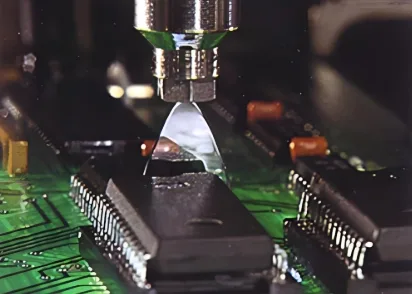
Principle: A thin layer of polymer film—such as acrylic, silicone, or polyurethane—is applied to the surface of the PCB by spraying, dipping, or brushing. This film covers all components and solder joints to form a protective layer.
Advantages:
-
Relatively low cost.
-
Easy to apply and suitable for a wide range of applications.
-
Minimal impact on the PCB’s heat dissipation.
Disadvantages:
-
Limited protection; not suitable for high-pressure water or long-term submersion.
-
The coating is thin and has average abrasion resistance.
-
Some types of conformal coating are difficult to remove for repair or rework.
2. Nanocoating
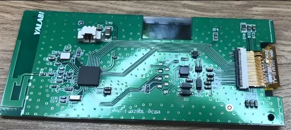
Principle: A molecular-level protective film is formed on the PCB surface using ultra-thin nanomaterials. This coating is superhydrophobic and repels water similarly to a lotus leaf.
Advantages:
-
Extremely thin coating that doesn’t alter the appearance or size of components.
-
Excellent waterproofing, moisture resistance, and corrosion protection.
-
Easy to apply, usually by dipping or vapor deposition.
-
Has virtually no effect on heat dissipation.
Disadvantages:
-
Lower abrasion resistance; the coating can be damaged by friction.
-
Relatively higher cost.
-
Best suited for products with high waterproofing requirements, but not ideal for prolonged submersion.
3. Potting
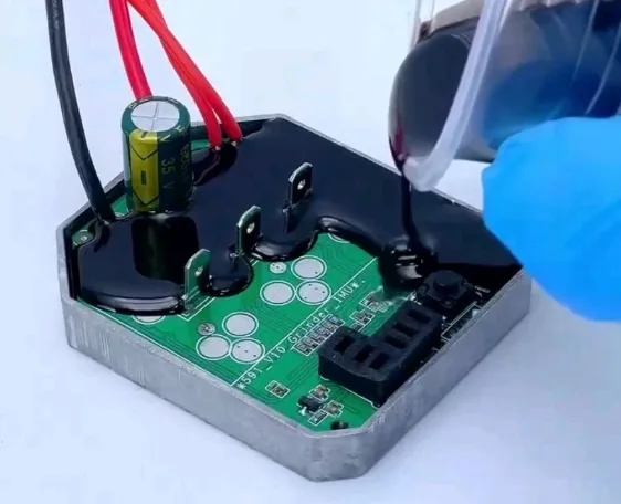
Principle: The entire PCB or critical areas are placed into an enclosure and filled with potting compounds such as epoxy, polyurethane, or silicone to completely encapsulate the components.
Advantages:
-
Offers the highest level of protection against water, dust, vibration, and corrosion.
-
Capable of withstanding prolonged submersion and harsh environments.
-
Also provides insulation and heat dissipation.
Disadvantages:
-
Non-repairable: once potted, internal components cannot be replaced or serviced.
-
Adds to the product’s weight and size.
-
Highest cost and more complex manufacturing process.
How to Waterproof Your PCB: Step-by-Step Guide
Waterproofing a PCB is a meticulous process that varies significantly depending on the chosen method. Below, we provide a detailed walkthrough of the specific procedures for the three most common waterproofing techniques: conformal coating, nanocoating, and potting.
1. Conformal Coating – Step-by-Step Process
Conformal coating is the most widely used method for waterproofing PCBs. It is relatively easy to apply, but requires careful attention to ensure even coverage.
Preparation:
-
Clean the PCB: This is the most critical step. The PCB surface must be completely clean and dry, free from dust, flux residues, oils, or fingerprints. Use a professional PCB cleaner and then blow dry with compressed air to ensure no moisture remains.
-
Mask off areas: Use high-temperature masking tape or special masking compounds to cover any areas that should not be coated, such as connectors, heat sinks, adjustable resistors, and test points. This prevents coating from interfering with their functionality.
-
Prepare the coating: According to the product instructions, stir or dilute the conformal coating to achieve the proper viscosity and uniformity.
Application:
-
Brushing: For small-batch production or rework, a brush can be used to manually apply the coating evenly. Control thickness and avoid bubbles.
-
Spraying: This is the most common method. Use a spray gun or automated system to apply the coating at a uniform speed and distance. Usually, two coats are applied: after the first layer is touch-dry (10–30 minutes), a second layer is added.
-
Dipping: Submerge the entire PCB vertically or at an angle into the coating, then slowly withdraw it. This ensures full coverage but requires special equipment.
Curing:
-
Surface drying: After application, allow the board to rest at room temperature until the surface is no longer tacky.
-
Full curing: Depending on the coating type (acrylic, silicone, polyurethane), allow it to air dry or use an oven to accelerate curing and enhance performance.
2. Nanocoating – Step-by-Step Process
Nanocoating is a high-tech waterproofing method that emphasizes cleanliness and precision.
Preparation:
-
Deep cleaning: Nanocoating requires extremely clean surfaces. In addition to standard cleaning, plasma cleaning is often used to activate the PCB surface and improve adhesion.
-
Dust-free environment: All steps must be carried out in a cleanroom or on a dust-free workstation to prevent particle contamination.
Application:
-
Dip coating: Submerge the cleaned and dried PCB into the nanocoating solution for a few seconds to a few minutes, then slowly remove it to avoid bubbles.
-
Vapor deposition: This advanced method uses specialized equipment to deposit the nanomaterial in vapor form, creating an ultra-thin, uniform coating.
Curing:
-
Natural curing: Most nanocoatings cure quickly at room temperature, typically within minutes to an hour, without the need for heat or baking.
3. Potting – Step-by-Step Process
Potting offers the highest level of protection but is more complex and non-reversible.
Preparation:
-
Clean the PCB: Just like with conformal coating, thorough cleaning is essential.
-
Choose the enclosure: Select a case or housing that matches the PCB dimensions and serves as the mold for potting.
-
Prepare potting compound: Most potting materials are two-part systems (Part A and Part B). Mix them according to instructions, ensuring a homogeneous blend.
Application:
-
Pre-potting: Pour a small amount of potting compound into the enclosure base.
-
Place the PCB: Insert the fully tested PCB into the enclosure.
-
Final potting: Slowly pour in the remaining compound until the PCB and all components are fully submerged. Pour steadily to avoid bubbles.
-
Vacuum degassing (optional): Place the potted assembly in a vacuum chamber to eliminate trapped air and bubbles.
Curing:
-
Curing: Let the potted product cure at room temperature or in an oven, depending on the material. Curing can take several hours or even a full day.
How to Choose the Right Waterproofing Method for Your Project
Selecting the right waterproofing method depends on multiple factors:
-
Protection level: What IP rating does your product need? For basic splash protection, conformal coating or nanocoating may suffice. For submersion or high-pressure water exposure, potting is more appropriate.
-
Budget: Potting is significantly more expensive than conformal or nanocoating. Choose based on your cost constraints and market goals.
-
Repairability: Will the product need maintenance or rework? Potting prevents any future repairs, while conformal coatings and nanocoatings are easier to remove and reapply.
-
Operating environment: Will the product be used indoors or outdoors? Is it exposed to humidity, rain, snow, salt mist, or corrosive gases? These conditions will influence material selection.
Conclusion
Waterproof PCBs are a critical part of modern electronic design. By leveraging conformal coating, nanocoating, or potting, you can provide tailored levels of protection to meet the specific demands of your application.