

Ultrasonic diagnostic device, also known as ultrasonic diagnostic device, is a instrument that uses ultrasonic diagnosis to diagnose medical diagnosis. Its working principle is to launch ultrasonic in the human body. When the ultrasonic wave encounters the interface in the body, reflection and reflection will occur, and may be absorbed and attenuated in human tissues. Due to the different shapes and structures of various tissues of the human body, the degree of reflection, refraction and absorption of ultrasound will be different. The doctor is based on the waveforms, curves, or imaging characteristics reflected by the instrument to distinguish these tissues, and combines anatomical knowledge and pathological changes to diagnose whether the organs checked are sick.
Ultrasonic diagnostic instrument is a medical research instrument for clinical medicine. Ultrasound medical imaging equipment can be divided into many types based on its principles, tasks and equipment systems.
1. Classification of space to obtain information
(1) One -dimensional information devices such as type A, M -type, and D.
(2) Two -dimensional information equipment such as fan -shaped scanning B, linear scanning type B, convex array scanning type B, etc.
(3) Three -dimensional information equipment is the three -dimensional ultrasound equipment.
2. Classification by ultrasonic waveform
(1) Continuous wave ultrasonic equipment such as continuous wave ultrasound polytele blood flow instrument.
(2) Pulse wave ultrasound equipment such as type A, M, and B ultrasonic diagnostic instrument.
3. Classification according to the physical characteristics of use
(1) Echo -type ultrasound diagnostic instrument such as type A, M, B, B, D, etc.
(2) Input ultrasound diagnostic instrument such as ultrasonic microscopes and ultrasonic holographic imaging systems.
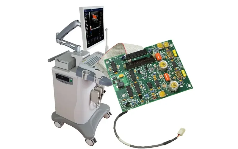
Silk printing process: Silk printing process is to print the circuit diagram to the circuit board to facilitate the subsequent welding process.
Drilling process: The drilling process is to drill on the circuit board with a drill bit to facilitate the welding of the components on the circuit board.
Patching process: Patching process is to install components on the circuit board to facilitate subsequent welding processes.
DIP plug -in welding process: The welding process is to welded the components on the circuit board with welding to facilitate the normal work of the circuit board.
Detection process: The detection process is to check whether there are defects in the circuit board to ensure the quality of the circuit board. Common AOI, SPI, etc.
If you think the reliability of PCBA is important, you can choose LST. LST has focused on providing high -reliability electronic assembly manufacturing services for 18 years. It mainly focuses on medical, new energy, automotive electronics, security, communication, AI artificial intelligence and other fields. Members of the core technology team have more than 20 years of experience in electronic product design, development and manufacturing industry experience. So far, it has provided high -reliable electronic assembly services for customers in more than 300 different industries worldwide in more than 40 countries and regions in the world.
| Number of layers | 1-48 layers |
| Materials | FR4, Tg=135150170180210, cem-3, cem-1, aluminum substrate, PTFE, Rogers, Nelco |
| Copper thickness | 1/2oz, 1oz, 2oz, 3oz, 4oz, 5oz |
| Board Thickness | 8-236mil (0.2-6.0mm) |
| Minimum line width/spacing | 3/3 million (75/75um) |
| Minute drilling size | 8 million (0.2 mm) |
| Min HDI laser drill size | 3 million (0.067 mm) |
| Aperture tolerance | 2 million (0.05 mm) |
| PTH copper thickness | 1 million (25 microns) |
| Resistance welding color | Green, Blue, Yellow, White, Black, Red |
| Strippable solder mask layer | yes |
| surface treatment | HASL (ROHS), ENING, OSP, sinking silver, sinking tin, shining gold, golden fingers |
| Gold thickness | 2-30u “(0.05-0.76um) |
| Blind hole/buried hole | yes |
| V-shaped cutting | yes |


