

PCB prototyping refers to the complete manufacturing process of converting a designed circuit layout (Gerber files) into a physical printed circuit board (bare PCB, without electronic components). It typically includes thirteen core stages: engineering data processing, material cutting, inner-layer circuit fabrication, lamination, drilling, electroless copper deposition and electroplating, outer-layer circuit fabrication, solder mask application, silkscreen printing, surface finishing, profile machining, electrical testing, and final inspection and packaging.
The specific processes vary slightly depending on the number of layers, such as single-sided PCBs, double-sided PCBs, and multilayer PCBs. However, the overall manufacturing logic follows the same sequence: first fabricate the inner-layer circuits → then laminate and drill to connect different layers → then fabricate the outer-layer circuits and apply surface finishing → finally perform board profiling and testing.
This article will break down the principles, key process parameters, and common issues involved in each manufacturing stage in production order. It will also include a comparison of surface finishing methods, common defect prevention measures, and key considerations for selecting a reliable PCB manufacturer.
I. Preparation Before PCB Fabrication: Engineering Data Processing (CAM/DFM)
After a PCB manufacturer receives the customer’s Gerber files, the first step is not to begin production immediately. Instead, the engineering team first processes and reviews the manufacturing data.
- File format standardization: Design files exported from different EDA software may use slightly different formats. The manufacturer converts them into a standardized Gerber RS-274X or Gerber X2 format.
- DFM inspection: Engineers verify whether parameters such as trace width and spacing, drill size, annular ring, and solder mask dam width meet the manufacturing capabilities of the production line. Potential design issues are identified in advance to avoid discovering problems only after production has started, which could result in board scrap.
- Panelization design: Based on the customer’s individual PCB dimensions and production efficiency requirements, the manufacturer determines whether to use V-Cut, mouse bites, routing slots, or other panelization methods (for more details, refer to A Complete Guide to PCB Panelization Methods). Process rails and fiducial mark locations are also designed during this stage.
Organizing the Manufacturing Parameter List Before Ordering
A complete set of manufacturing parameters should be prepared before placing an order to avoid missing process selections that could result in PCB scrap:
- Number of layers: Single-sided PCB / double-sided PCB / 4-layer / 6-layer and other multilayer PCBs
- PCB material: Standard FR-4, high-Tg material, aluminum-based PCB, Rogers high-frequency PCB, etc.
- Board thickness and copper thickness: 1 oz / 0.5 oz
- Solder mask color: Green, black, red, blue, etc.
- Surface finishing process: HASL, ENIG, OSP, immersion silver
- Special requirements: Impedance control, via filling, via-in-pad, gold fingers
- Quantity: A few prototype boards or a small batch of several hundred boards
- Panelization and testing requirements: Flying probe testing / AOI optical inspection
Although this stage does not directly produce the physical PCB, it is a critical preliminary step that determines whether subsequent mass production can proceed smoothly and whether production yield can remain stable. Many rework issues during the prototyping stage can ultimately be traced back to insufficient DFM inspection at this stage.
II. Material Cutting
Material cutting is the process of cutting a full sheet of copper-clad laminate (CCL) into working panels according to the required production dimensions.
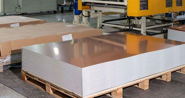
This stage introduces several basic concepts:
- UNIT: The individual board design created by the engineer, representing one actual PCB product.
- SET / PANEL: A complete layout created by arranging multiple UNIT boards together according to panelization rules in order to improve production efficiency. This is the panelization mentioned earlier.
The cutting dimensions and accuracy directly affect the positioning references used in all subsequent manufacturing processes and serve as the starting point of the entire PCB production workflow.
III. Inner-Layer Circuit Fabrication (Exclusive Process for Multilayer PCBs)
Single-sided and double-sided PCBs do not require this stage. However, multilayer PCBs with four layers or more must first have the circuits fabricated separately on their inner-layer core boards.
The specific process includes:
- Surface preparation: The copper-clad laminate surface is cleaned and roughened to improve the bonding strength between the copper surface and the dry film.
- Dry film lamination: Photosensitive dry film is uniformly laminated onto the copper foil surface.
- Exposure: The designed circuit pattern is transferred onto the dry film through a phototool (film artwork). The exposed areas undergo a curing reaction.
- Development: Developer solution is used to remove the unexposed dry film, exposing the copper areas that need to be etched.
- Etching: Chemical solutions are used to dissolve the copper that is not protected by the dry film, leaving only the required circuit pattern.
- Dry film stripping: The remaining dry film is removed to expose the final inner-layer copper circuits.
- Inner-layer AOI inspection: Automated optical inspection is used to check whether the inner-layer circuits contain defects such as open circuits, short circuits, or abnormal trace widths. Unqualified core boards are intercepted at this stage to prevent them from entering the subsequent lamination process and causing greater material waste.
IV. Lamination
For multilayer PCBs, the fabricated inner-layer core boards, prepreg (PP), and outer-layer copper foil are stacked according to the designed layer sequence and then placed into a lamination press. Under high temperature and high pressure, they are bonded together into a single structure.
The prepreg melts and flows at high temperatures, filling the gaps between circuit patterns. After cooling, it cures and firmly bonds multiple core boards together into a complete multilayer PCB substrate.
Lamination parameters, including the temperature profile, pressure, and processing time, directly affect the risk of delamination and the layer-to-layer alignment accuracy of the finished PCB. Therefore, lamination is one of the key stages in multilayer PCB quality control.
V. Drilling
After lamination, precision CNC drilling machines are used to drill various types of holes in the PCB for interlayer connection, component mounting, or mechanical fixation.
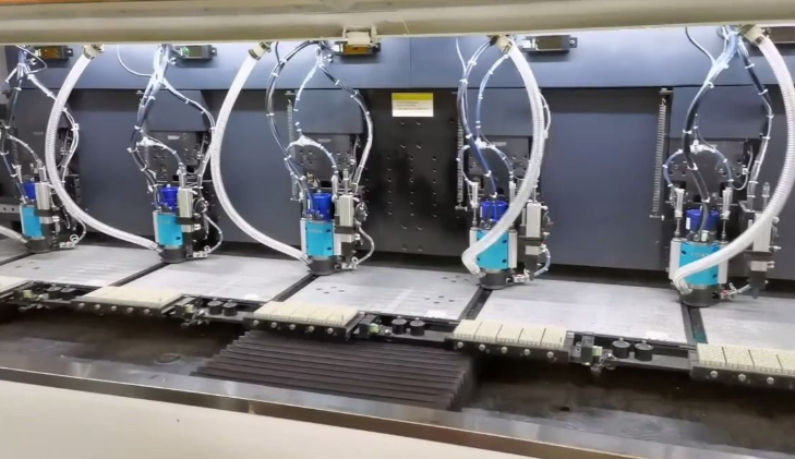
Common hole types include:
- Through Hole: Extends through the entire PCB and can provide electrical connections between any layers. It is the most common and lowest-cost type of hole.
- Blind Via: Connects only an outer layer to a specific inner layer and does not extend through the entire board. It is commonly used in HDI (High-Density Interconnect) PCBs.
- Buried Via: Completely embedded between inner layers and invisible from the PCB surface. It is mainly used in high-density multilayer PCBs.
- Mechanical Drilling and Laser Drilling: Conventional hole sizes are typically processed using mechanical drill bits, while microvias, especially blind vias, are often produced using laser drilling to achieve higher precision.
After drilling, the hole walls essentially consist of non-conductive resin and glass fiber materials. Therefore, metallization is required in the next step to provide electrical conductivity.
VI. Electroless Copper Deposition and Electroplating (PTH, Plated Through Hole)
The hole walls after drilling are made of insulating materials. To make them conductive and electrically connect the circuits between different layers, the hole walls must first undergo electroless copper deposition, which deposits an extremely thin layer of chemical copper, followed by copper electroplating to increase the copper thickness.
This process is known as PTH (Plated Through Hole) and provides the physical foundation for interlayer electrical connections in multilayer PCBs.
Uneven electroless copper thickness or voids in the copper layer are common causes of subsequent reliability issues, such as hole wall cracking and interlayer open circuits. Therefore, this process is also one of the key inspection items in PCB quality control.
VII. Outer-Layer Circuit Fabrication (Pattern Plating Process)
The manufacturing logic of the outer-layer circuits is similar to that of the inner layers, including dry film lamination, exposure, and development. However, the Pattern Plating process is typically used.
First, the copper layer is electroplated and thickened in the areas where the circuit patterns need to be retained. A layer of tin is then plated as an etching protection layer. The excess copper is subsequently etched away, and finally, the tin protection layer is stripped to expose the finished outer-layer circuit patterns.
Compared with the direct etching method used for inner-layer circuits, pattern plating can better ensure the consistency of copper thickness between plated through holes and circuit traces.
VIII. Solder Mask (Commonly Known as “Green Oil”)
After circuit fabrication is completed, a layer of solder mask ink is screen printed or applied through exposure onto the PCB surface. The solder mask covers all copper areas except the solder pads.
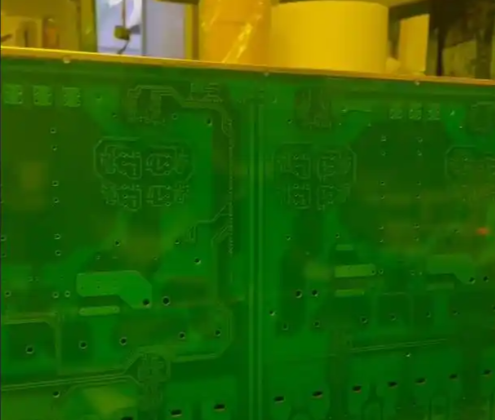
Although green is the most common color, solder masks are also available in blue, red, black, white, and other colors.
The functions of the solder mask include:
- Preventing adjacent circuits from accidentally forming solder bridges and short circuits during soldering;
- Protecting copper traces from oxidation and environmental corrosion;
- Providing basic electrical insulation.
The solder mask dam width, which refers to the minimum width of solder mask ink between adjacent pads, is one of the key parameters checked during DFM analysis. If it is too narrow, solder mask peeling or solder bridging problems may occur during production.
IX. Legend Printing / Silkscreen
Component reference designators, polarity markings, product models, production batch information, and other text or symbols are printed on the PCB surface.
These markings make it easier to quickly identify component locations and orientations during subsequent SMT assembly, mechanical assembly, and maintenance. They serve as production and identification information and do not perform an electrical function.
X. Surface Finish
Bare copper is highly susceptible to oxidation when exposed to air, which can affect solderability. Therefore, the pad areas require surface finishing.
Common surface finishing methods are compared below:
| Surface Finish | Features | Typical Applications |
|---|---|---|
| HASL (Hot Air Solder Leveling) | Low cost and good solderability, but relatively poor surface flatness; not suitable for fine-pitch assembly | Conventional consumer electronics and cost-sensitive products |
| Lead-Free HASL | Environmentally compliant, with slightly better flatness than leaded HASL | Products required to comply with environmental regulations such as RoHS |
| ENIG (Electroless Nickel Immersion Gold) | Excellent surface flatness, solderability, and oxidation resistance; suitable for fine-pitch BGA/QFN components | High-density assembly and products requiring long-term storage |
| Immersion Silver | Good electrical conductivity and lower cost than ENIG, but has a certain risk of oxidation and discoloration | Applications with relatively high signal integrity requirements |
| OSP (Organic Solderability Preservative) | Low cost and good surface flatness, but relatively short storage life; solderability decreases after multiple reflow cycles | One-time assembly and products with short production turnover cycles |
The selection of a surface finishing method should take into account factors such as assembly accuracy requirements, storage period, cost budget, and whether multiple rework or reflow processes will be required.
XI. Profile Machining (Board Profiling)
According to the designed PCB outline, the panel is cut and separated into the final individual board shape by routing (CNC milling) or stamping. At the same time, panel connection structures such as V-Cuts and mouse bites are processed.
If the PCBs are delivered in panels, the panel connection structures will be retained during this step and separated later by the customer or during the downstream SMT assembly process.
XII. Electrical Testing
After board profiling is completed, each PCB needs to undergo continuity and isolation testing to confirm whether defects such as open circuits or short circuits are present.
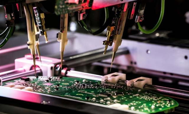
Common testing methods include:
- Flying Probe Testing: No dedicated test fixture is required. Moving probes are used to test individual points on the PCB. This method is suitable for prototyping and small-batch production.
- Bed-of-Nails Testing: A dedicated test fixture is required, but testing efficiency is higher, making it suitable for mass production.
XIII. Final Inspection, Sampling Inspection, and Packaging
Finally, a visual inspection is performed to check items such as board dimensions, warpage, and solder mask quality. Sampling inspections are conducted according to the required sampling ratio to confirm the overall production yield.
The PCBs are then packaged according to customer requirements with moisture-proof and anti-static protection before shipment.
At this point, the complete manufacturing process of a bare PCB is finished. The boards can then proceed to the SMT assembly stage to become PCBA products.
XIV. Comparison of Manufacturing Process Differences for Different PCB Types
| PCB Type | Key Process Differences |
|---|---|
| Single-Sided PCB | Material cutting → drilling → outer-layer imaging → etching → solder mask printing → (HASL) → legend printing → profile machining → testing → inspection. No lamination or electroless copper deposition is required. |
| Double-Sided PCB | Electroless copper deposition/electroplating is added to achieve electrical connections between both sides. Other processes are similar to those used for single-sided PCBs. |
| Multilayer PCB | Inner-layer circuit fabrication must first be completed, followed by the full process of lamination, drilling, electroless copper deposition and electroplating, outer-layer circuit fabrication, and other processes. It has the most complex manufacturing process and the longest production cycle. |
| HDI (High-Density Interconnect) PCB | Based on the multilayer PCB process, laser drilling is added to produce blind and buried vias, with higher requirements for drilling accuracy and layer-to-layer alignment. |
XV. Common Defects During PCB Fabrication and Prevention Measures
| Defect | Common Causes | Prevention Measures |
|---|---|---|
| Delamination / Blistering | Improper lamination temperature profile or insufficient heat resistance of the PCB material | Set lamination process parameters appropriately according to the Tg value of the material |
| Hole Wall Voids / Poor Electroless Copper Deposition | Unstable electroless copper process control or insufficient hole wall roughening | Strengthen process control during electroless copper deposition and perform cross-section sampling inspections |
| Incomplete Etching / Residual Copper on Circuit Areas | Improper control of etching solution concentration or processing time | Regularly calibrate etching parameters and combine them with 100% AOI inspection |
| Solder Mask Blistering / Peeling | Solder mask dams designed too narrow or uneven screen-printing thickness | Reserve sufficient solder mask dam width during the design stage and control printing uniformity during production |
| Hole Position Deviation | Errors in drilling positioning references or insufficient compensation for thermal expansion and contraction of the PCB material | Use precision optical positioning fiducials and control the temperature and humidity of the drilling environment |
XVI. Key PCB Prototyping Parameters, Cost Factors, and Lead Time Reference
1. Lead Time Reference (General Industry Standards for 2026)
- Standard double-sided PCB prototypes: 3–5 working days; expedited service: 24–48 hours
- 4-layer PCBs: Standard lead time of 5–7 days
- 6–8 layer PCBs: 7–10 days
- High-frequency materials, impedance control, via-in-pad, and resin-filled vias: An additional 2–4 days
Note: During holidays or at the end of the month, factory production capacity may be fully booked. Even expedited orders may experience delays. For important projects, it is recommended to avoid placing orders during peak production periods whenever possible.
2. Key Factors Affecting PCB Prototyping Prices
- PCB material type: FR-4 is generally the lowest-cost option, while Rogers materials and aluminum-based PCBs are significantly more expensive.
- Number of layers: The more layers a PCB has, the higher the unit price.
- Copper thickness and board thickness
- Surface finish: ENIG > HASL > OSP in terms of general cost.
- Special processes: Impedance control, via filling, via-in-pad, and gold fingers usually involve additional process charges.
- Order quantity: Individual prototype boards have a higher unit cost, while larger small-batch quantities generally reduce the cost per board.
Conclusion
PCB prototyping is a closely connected manufacturing process in which every stage affects the next. Inner-layer circuits determine the fundamental electrical performance of multilayer PCBs, while lamination and drilling determine the reliability of interlayer connections. Surface finishing and outer-layer circuits are directly related to the assembly yield of subsequent SMT processes.
Understanding the principles and common risk points of each process can not only help you proactively avoid redesign and rework during the PCB design stage, but also give you greater confidence when evaluating a manufacturer’s capabilities and determining whether a quotation is reasonable.
The core principle can be summarized as follows: the more complex the PCB structure—such as having more layers or including blind and buried vias—the longer and more complicated the manufacturing process becomes, and the higher the requirements for process control and upfront DFM inspection.